Technology coverage
Mature node
specialists
We operate exclusively at 28nm and above — the sweet spot for analog/RF, mixed-signal, and cost-efficient digital designs.
28nm
LP / HPC
40nm
LP / G
65nm
LP / G
90nm
General
130nm
HV / BCD
180nm
Analog / HV
350nm+
Power / HV
Compatible foundries
TSMC
GlobalFoundries
SMIC
UMC
Tower Jazz
DB HiTek
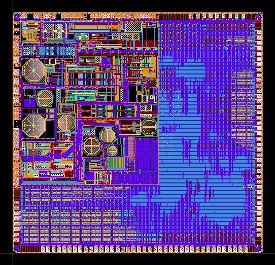
layout_top.gds — 6-Metal (TSMC 55nm)